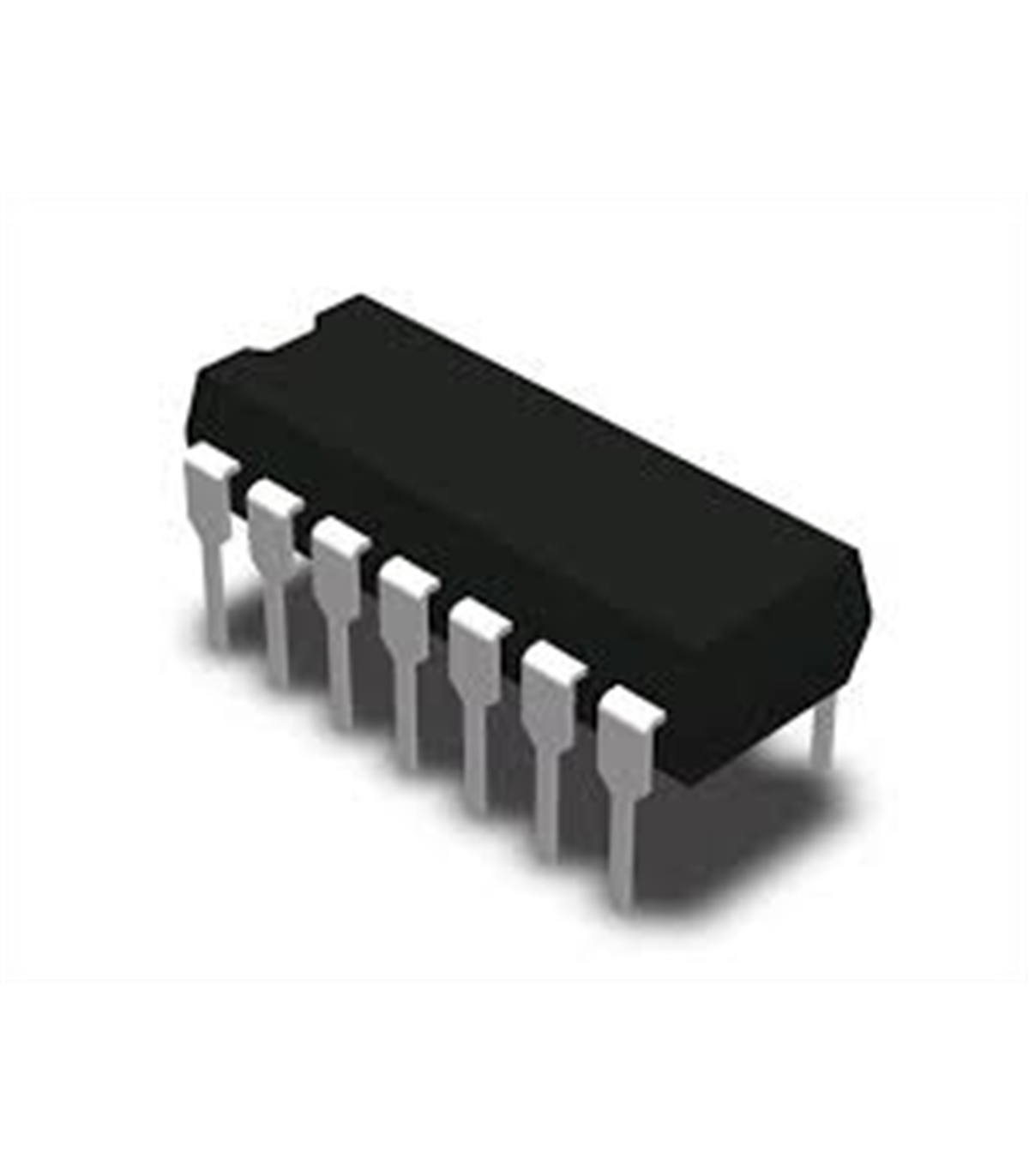
CD74HCU04 - Hex Unbuffered Inverter
Features
• Output Drive Capability: 10 LSTTL Loads
• Outputs Directly Interface to CMOS, NMOS, and TTL
• Operating Voltage Range: 2.0 to 6.0 V; 2.5 to 6.0 V in Oscillator
Configurations
• Low Input Current: 1.0 mA
• High Noise Immunity Characteristic of CMOS Devices
• In Compliance With the JEDEC Standard No. 7.0 A Requirements
• ESD Performance: HBM > 2000 V; Machine Model > 200 V
• Chip Complexity: 12 FETs or 3 Equivalent Gates
• These are Pb-Free Devices
http://html.alldatasheet.com/html-pdf/314547/ONSEMI/74HCU04/216/1/74HCU04.html